In short
Eye On A.I. Podcast Episode #223 Summary
Episode Title
Kai Beckmann: Why Next-Gen Chips Are Critical for AI's Future
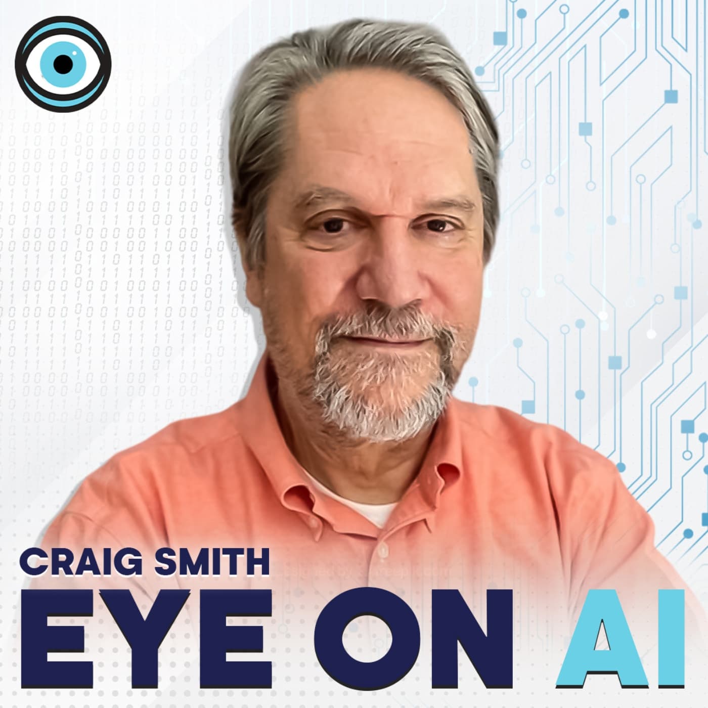
Episode Description In this episode, Craig Smith engages with Kai Beckmann, CEO of Merck KGaA, to delve into semiconductor innovation and its significance in the future of artificial intelligence (AI). Beckmann discusses the intricate processes involved in chip manufacturing and how advances in materials science are essential for the evolving demands of AI technologies.
Key Topics Discussed
- Introduction to Merck KGaA
- Company Origins: Founded in the late 17th century, Merck KGaA is distinct from the American pharmaceutical Merck, operating primarily in healthcare, life sciences, and electronics.
- Role in Semiconductor Manufacturing: The company is a leading provider of specialty materials essential for semiconductor production.
- Foundations of Semiconductor Manufacturing
- Manufacturing Process: Overview of how semiconductors are made, including steps like photolithography, thin film deposition, and etching.
- Complexity of Modern Chips: Modern chips can contain over 100 billion transistors, necessitating advanced materials and technologies.
- The Impact of AI on the Semiconductor Industry
- Growing Demands: AI technologies require increasingly sophisticated semiconductor designs, including edge AI and heterogeneous integration.
- Material Science Innovation: Merck is pioneering new materials that enhance chip performance and capabilities.
- Trends and Growth in Semiconductor Industry
- AI-Driven Growth: The demand for high-performance chips due to AI applications is reshaping how semiconductors are manufactured.
- Cyclical Nature of Industry: The semiconductor industry experiences cycles of boom and bust, influenced by factors such as inventory levels and technological advancements.
- AI in Material Discovery
- Accelerated Research: AI significantly reduces the time and resources needed for material discovery, enhancing innovation speed.
- Successful Experimentation: By using AI, the company can eliminate non-viable experiments, enabling chemists to focus on successful outcomes.
- Continued Evolution of Semiconductor Fabrication
- 3D Structures and Chiplets: Future chip designs may leverage chiplets and 3D stacking to improve performance without purely relying on traditional miniaturization methods.
- Material Innovations: Exploring new conductive materials and refining manufacturing processes to address energy consumption and latency issues.
Key Takeaways
- The semiconductor industry is entering an "Age of Materials," where material science is pivotal to advancing AI and other technologies.
- Merck KGaA plays a critical role in providing materials that underpin the semiconductor manufacturing process, showcasing the company's extensive involvement across the entire industry.
- The integration of AI in both semiconductor design and material discovery is transforming how the industry operates, leading to faster innovation cycles and more efficient production processes.
Future Outlook
- As AI continues to expand, the demand for next-generation chips will increase, prompting further research and development in materials and manufacturing techniques.
- The semiconductor industry’s growth trajectory looks promising, with significant advancements anticipated in the coming years, driven by AI and new technologies.
Additional Information
- Sponsor: The episode is sponsored by NetSuite by Oracle, a cloud financial system designed to streamline business processes.
Stay Connected
- Craig Smith Twitter: [@craigss](https://twitter.com/craigss)
- Eye on A.I. Twitter: [@EyeOn_AI](https://twitter.com/EyeOn_AI)
Episode Timestamp Breakdown
- 00:00 - Introduction
- 02:48 - Overview of Merck KGaA
- 05:21 - Foundations of Semiconductor Manufacturing
- 07:57 - How Chips Are Made
- 09:24 - Exploring Materials Science
- 13:59 - Growth and Trends in the Semiconductor Industry
- 15:44 - Semiconductor Manufacturing
- 17:34 - AI's Growing Demands on Semiconductor Tech
- 20:34 - The Future of Edge AI
- 22:10 - Using AI to Disrupt Material Discovery
- 24:58 - How AI Accelerates Innovation in Semiconductors
- 27:32 - Evolution of Semiconductor Fabrication Processes
- 30:08 - Advanced Techniques: Chiplets, 3D Stacking, and Beyond
- 32:29 - Merck's Role in Global Semiconductor Innovation
- 34:03 - Major Markets for Semiconductor Manufacturing
- 37:18 - Challenges in Reducing Latency and Energy Consumption
- 40:21 - Exploring New Conductive Materials for Efficiency
This comprehensive summary encapsulates the key discussions and insights from the episode, highlighting the pivotal role of semiconductor materials in the AI landscape and the future of technology.
Written by AI. May contain mistakes. Listen to the episode to check what was said.
Transcript
Automatic transcript. May contain errors.0:00AI boom is defined by building capacity in data centers for training large language models. Current application is more you use a web interface, you do chat GPT and use the large language model. What is still to come is H-AI. I mean, you put an AI chip on a smartphone, take the latest iPhone, and then you can do inference on the AI models right on your end device. You don't need to transfer data like crazy up and down the cloud. What does the future hold for business? Ask nine experts and get 10 answers. Bull market, bear market, rates rising or falling, inflation going up or down. Can somebody please invent a crystal ball?
0:43Until then, over 40 ,000 enterprises have future-proofed their business with NetSuite by Oracle, the number one cloud ERP, bringing accounting, financial management, inventory, HR into one fluid platform. With one unified business management suite, there's one source of truth, giving you the visibility and control you need to make quick decisions. With real-time insights and forecasting, you're peering into the future with actionable data. If I were a larger organization, this is the product I'd use. Whether your company is earning millions or even hundreds of millions, NetSuite helps you respond to immediate challenges and seize your biggest opportunities.
1:37Speaking of opportunities, download the CFO's Guide to AI and Machine Learning at netsuite.com slash ionai. That's netsuite, N-E-T-S-U-I-T-E dot com slash ionai, E-Y-E-O-N-A-I, all run together to get the CFO's Guide to AI and Machine Learning. The guide is free to you at netsuite.com slash IonAI. netsuite.com slash IonAI. I generally start by having you introduce yourself and how you became CEO of the electronics business of Merck, KGAA, in Darmstadt, Germany. and then we'll talk about material science and semiconductors and all of the businesses that you have that impact artificial intelligence.
2:48Yeah, Greg, thanks a lot for having me on the podcast. So my name is Kai Beckman, so I started in our company already more than 35 years ago. I'm a computer scientist by training. I did a minor on microelectronics, so the interest for semiconductors is deeply rooted in myself. I then had opportunities to work in all areas of our company. In IT, I was leading HR, I was in the countries running our businesses in Singapore and Malaysia, healthcare business, life science performance material business. And then I entered the executive board some meanwhile, 13 years, 13 years ago, and being in charge of a number of what we call group functions, HR procurement, our major production side, our headquarters side, as well as as many other functions.
3:47And then seven years ago, I was asked to take over performance materials, performance materials business, which we have then rebranded a while ago as electronics, based on our transformation away from a materials business to an integrated solution provider for the electronics industry and specifically for the semiconductor industry. Can I just say, just for listeners who might be confused, Merck KGAA is a German company. It was founded by Jacob Merck, I think, in the late 17th centuries, or Friedrich Jacob Merck. And that company then split eventually between the Merck that Americans know, which is the big pharmaceuticals company, and your company.
4:50So they're two separate companies. I think Americans can easily get confused by that. Absolutely. And thanks for explaining that. So we have a more than 350 years history as the kind of Germany headquartered company. And so we operate in three different businesses. We operate in healthcare, we operate in life sciences, as well as in electronics. So covering a broad spectrum of different industries and different technologies and science. Yeah. Can you tell me about the work that you do that is foundational to semiconductors? Yeah. As I said, our roots are in chemistry, our roots are in biology, our roots are in physics.
5:36And if you combine physics and chemistry, then you easily kind of reach the field of materials, specialty materials for the electronics industry. And since we started the transformation towards electronics, we combine different parts into our portfolio, different parts across different technology steps, manufacturing steps of making semiconductors from delivery systems in a subfab that make chemistry gases available to the tools, to materials across the full production cycle of semiconductors, from patterning to cleans to glenarization, thin film materials, specialty gases. And so we offer a full spectrum, including with the latest acquisition of Unity SC, including metrology instruments for hydrogenous integration, which is very important and of new technology required to enhance the performance and the capability of semiconductor.
6:40In the semiconductor manufacturing process, is that too complicated to walk us through and tell us where in the process these Merck products come into play? That's a great point. So typically you start with like a blank wafer. A wafer doesn't come from us. There are other companies who supply the silicon wafer. And you start processing the wafer. so you start kind of patterning structures on a wafer this is a lithography step i mean you use uh light in today's world uh extreme ultraviolet um light to to create in a photo lithography step structures then with that kind of you wash off the unexposed parts of that you then build structures on that with thin film deposition on a wafer.
7:37And you start planarizing structures in order to get an even surface. You deposit materials to get kind of charged areas on a device positively or negatively. And then with that, you build these semiconductor transistors on a chip. And with that, then with these steps, more than a thousand, meanwhile, in most advanced technologies, more than a thousand steps, you build these enormously complex devices that can probably host more than 100 billion transistors on one chip in structure sizes that go well down to 2 nanometers scale. And that's kind of a technology which has advanced over the past years, dramatically in a way the level of complexity the level of performance has been accomplished and you need specialty materials to to create these highly highly complex and differentiated devices that's the way they want if you want to kind of a pretty pretty kind of visual number so if you take our materials and our technologies our equipment and our instruments so and if you try to identify in a normal retail store, electronic devices in a retail store, whether they have been exposed to our equipment or materials, there's a greater than 99 % probability that any electronic device, TV, handphone, computer, cars, what have you, has been made with the help of our materials, tools and equipment.
9:19And in terms of materials, those are layers on the silicon substrate that you're building up as you create the... What's the most common of those materials or the most heavily used? When I started doing that at university, and you had a handful of materials that you could use to make a semiconductor. And of course, silicon is the base material. And you have created silicon oxide layers for insulation. You have used aluminum for conducting layers. And that's basically kind of the set of materials. And you needed a couple of solvents to wash stuff off the surface. And that's about it. Meanwhile, we use 80 % of the non-radioactive periodic table of elements to make semiconductors.
10:1580%. There's not much left, Craig, on, let's say, advancing technology. There's a famous quote that was used publicly in many instances by Pat Gelsinger, CEO of Intel, who said, we're not going to stop innovating semiconductors until we have exploited the full periodic table of elements. This is music to my team's ears. So of course, for our chemists, that is the message that drives them to the next level of excitement and performance. And this is what feeds their brain for making better semiconductors tomorrow. And who are your principal clients in the semiconductor industry? Is it obviously TSMC, or are they component suppliers to the big foundries?
11:08So everyone who makes a semiconductor is on our client list. We have done a precise analysis. We took the top 100 companies who make semiconductors, and each one of them is on our client list, each one of them and of course typically these are companies who have fabs so not the fabless companies they're of course they give their um kind of manufacturing to to foundries companies who operate fabs in some instances the the tool companies can be customers too so they offer them fully packaged solutions uh to to our our fab customers but mainly it is the semiconductor semiconductor industry, which is on our client list.
11:55Yeah. And I have to ask, you know, I've spent a lot of my life in China, so I follow the China story. Are you guys restricted under the export controls to sell to China, or do your materials fall outside of that? Well, certainly we are restricted and we follow those restrictions very tightly and clearly. So we operate under all these kind of global rules and special national rules. I think we have to, of course, understand that we serve the display market as well, and 70 % of the global display real estate, so all display surface, is produced in China, 70%. And so there is almost 70 % of smartphones, TVs, automotive displays, they all come from China.
12:53So this is, of course, the lion's share of our activities in China, for China. Yeah. And in the business generally, is it the display business or the semiconductor business or something else that's the bulk of your business? The bulk is semiconductor, clearly. The majority, the vast majority of what we call electronics core, because we have put one part of our business, a surface solutions business, is for sale. And this has been already a signed deal and it's been carved out. So of what we call electronics core, the rest is already 80 percent is facing the semiconductor industry. And only then 20 percent is left for the display industry.
13:33Yeah, so you guys have a really wonderful overview of the semiconductor industry, right? Where is it growing? Is it growing everywhere? Is it, I mean, famously TSMC and Intel are building big fabs in the United States. Where is it growing right now? Any semiconductor industry is probably one of the most fascinating industries. And if anyone has any problems with blood pressure to work in a cyclical industry, maybe is not a good, not a good advice. So it's going up and down. It's like if you take my 35 years, if you take an average, it's like four good years, and then will be four bad quarters.
14:21This is the typical, typical cause of things. And it's always been like this. Now, meanwhile, it's getting a bit more complicated because different technologies have different cycles and they're not fully in sync like they were in the past. And this is why at any given point in time, there are some businesses, of course, beautifully developing and others are a bit more behind. In the current setup, of course, artificial intelligence drives a lot of crows in the semiconductor industry. And this is still predominantly focused on training large language models and the GPUs and the boards used in data center applications.
15:03This is driving a lot of growth as we speak. But other technologies, meanwhile, catching up slowly as well. But it's not anymore like as nice of a wave that you could monitor. It's more like many waves on top of one another. So the industry is a bit more kind of spread out in terms of recovery than it was in the past. That cyclical nature previously, was that tied to simply inventory piling up and then getting used and piling up? Or was it tied to some other cycle in the economy? If you look over a larger period of time, then predominantly it's driven by the fact that these fabs can run either fully utilized or they will be stopped.
15:53Lines will be stopped. And there is no such thing as a 50 % utilization typically in a simplified way. Just a simplified picture. so it means they run 100 and you create at some point inventory and you feel maybe now it's time to stop producing i need to deplete my inventory and then it goes comes all over again that is the simplified picture of course you can still find that in memory where the products are a bit more commoditized you find it less and less in logic where the the products are much more specialized on for different different customers. So this is why the picture is not anymore as it was in the past, you know, the cycles in the early 2000s, where even the logic party, the CPUs for desktop computing, where kind of almost commoditized, maybe the wrong word, but they were more replaceable than they are today.
16:51So in those times, it was piling up inventory and then depleting inventory again, is created the cycles and it's still the situation that these fabs can run either kind of on a full utilization or you better stop them because you're just burning cash. Yeah, although given the advance of AI and the demand generative AI and the demand for GPUs and the shortage in GPUs, it seems that that inventory buildup build-up is for the foreseeable future not going to be a problem. Is that right? That is a pretty steady demand. Yeah, still bear in mind that AI is in terms of percentage of all devices, semiconductor devices produced in the world is still a fairly low percentage.
17:43We are still talking about a fraction of a percent. So that's why it doesn't really move the needle in terms of overall capacity inventory yet in terms of value you're already reaching 10 percent of ai related semiconductor devices which of course includes not only the data center devices it includes as well kind of edge ai devices like yeah processors on a smartphone processes on a on a on a on for for mobile computing at large so this is the broader spectrum 10 of the value equals somewhere 4.1 or 2.2 % of the devices manufactured. How do you see that developing? Because certainly demand AI is going to spread.
18:29And are you guys, is that triggering any sort of shift in your production or triggering any sort of research for new materials that can be applied? I think the first thing it does, the kind of the AI boom that we see is it requires more sophisticated chips. That's what it does in the first place. So and more sophisticated by an order of magnitude, not just by a small margin. More complex architectures, smaller structure sizes, even what we call heterogeneously integrated semiconductor devices. it means you take chiplets and kind of glue them together in order to increase performance and and packaging density so that's of course again a dimension that helps kind of accelerating our contribution to to the industry that's the first thing the second thing is uh with the current uh yeah ai boom is defined by by building capacity in data centers for training large language models then the current application is more you use a web interface you do chat GPT and use the large language model what is still to come is edge AI you mean you put a chip on on a smartphone take the latest iPhone you have that functionality on the iPhone already but of course the percentage market share is not not huge yet and then you can do inference on the AI models right on your and device you don't need to transfer data like crazy up and down the cloud you can do that entrance on your device you mean things like microsoft copilot for example on a laptop computer can be done right on your on on your laptop computer with kind of an a cpu gpu that you have in order to do the inference that is the next level of of of ai use cases and i think we will all see that coming one could ask what is the killer app what will what will make that happen we shall see there's a lot being done around visualizing data analyzing data text analysis of course is a big deal there as well picture editing is an important area as well information research is an important part i i would suspect that a lot of these applications will be more and more compelling in their use case that demand for compute power, edge AI compute power on your end device will be increasing.
21:19Yeah. So you see your business growing dramatically, I guess, in the next 10 years. Yeah, we just upgraded our capital market guidance, midterm guidance based on those trends. Yes, I think we do have quite some confidence in the industry picking up on, driven by AI, the increased complexity of the chips as well as the sheer volume over the next couple of years. Absolutely. Yeah. And you guys develop new materials. Can you talk about what you're doing there? And obviously, AI is being applied to material science and discovering new materials. Do you guys use AI in your research? Great point. That's an amazing point.
22:12Of course, we enable AI and we use AI to enable us. So it's kind of a full circle of things. So the way, of course, we need to identify new molecules, new precursors that are used for making chips requires typically a lot of experiments where you check whether this precursor does what it's supposed to do. Can you synthesize it? Is it stable enough? Does it have the properties that you need? And with AI, we can reduce the number of necessary experiments quite drastically. So in a recent talk, I have explained that out of 100 different potential target molecules, we can remove 99 just based on AI and just synthesize one for the next level of testing.
23:07And then this next level of testing, that's another capability that we have built over the past five years. In the past, we would have provided then this kind of synthesized molecule to a tool company or to a semiconductor fab in order to test the electrical properties. Meanwhile, we have the same capability within our own premises. It's called intermolecular. It's a facility that's based in the Silicon Valley in San Jose. And so we then can do electrical combinatorial testing of that material on a wafer in a transistor structure. And with that, it used a cycle of these refinements of our material drastically.
23:55In the past, we talked about one to two years. And now we are in a week's scale. That's of course a huge benefit. Less experiments and faster cycle time is quite exciting. Of course, a pretty natural question that I typically get is that do our chemists like that? Because if they do less experiments, do they lose their jobs? I think it's the opposite because chemists, and I've talked to many of them, they like to do successful experiments. They don't like to do experiments that fail. And we remove the experiments that fail by artificial intelligence. Yeah. And that pace of discovery, is that resulting in new products for you guys?
24:42Absolutely. It is then identifying new material opportunities for our customers, which they then validate in their processes, which then feeds novel technologies that is then implemented by our customers. Yeah. I'm just curious. So when you synthesize a new molecule and you send it to California, in what form is that sent? Is that, I don't know, is it a vial of liquid? Is it a roll of sheet? Is it a block of solid material or is it just a formula? So it could be all of the above except the formula. So it's either it could be a liquid, a gas or a powder, a solid material. And it's shipped in, of course, containers, small containers that keep that intact and ensure safety for transportation.
25:48But that's the way how we handle these materials. Yeah, absolutely. Yeah. And then when you validated it, you put it into production for semiconductor fabs. And how often do you come out with new materials for semiconductor fabrication? It's pretty tough to give you a precise number because overall, our product list probably has a couple of thousand different different different materials material combinations molecules formulations and it's quite a frequent event that a new process step requires a new formulation a new precursor for for our customers so it's it's it's not just once a year it happens quite quite frequently not everything will be then adapted for mass production and but But still, it's a pretty normal, if not daily process.
26:48Wow. And do you see the semiconductor fabrication process changing, you know, in the next 10 years? I mean, I don't know if it's been the focus, but from my point of view, from a journalist's point of view, the focus has been on, you know, smaller and smaller gate sizes, as you said, down to two nanometer. Is it going to continue miniaturizing or are there gains to be had through other parts of the process, maybe through materials? Yeah, that's a great point. So, you know, when I was at university at the end of the 80s of the last century and already many people speculated, is Moore's law over?
27:43that was you know it's quite a while quite a while ago and so maybe half jokingly we have said there's maybe like a derived Moore's law that the number of people declaring Moore's law being over doubles every other year so that's
28:02I didn't get a trademark for that so it's it's free to use that they certainly not for Beckmann's law I can tell you but so the the dimension the the focus was on on what we call shrink so getting the geography to to to create smaller structures and everything else was auxiliary to to making a semiconductor over a couple of decades over about two three decades now and of course we are we are touching limits there may be physical limits but more importantly there economic limit limits to that where it simply it doesn't scale financially properly and this is where then additional um uh methods are being used and probably the most the most um uh yeah novel way of doing it is uh the current trend especially in the area of ai uh around heterogeneous integration so you build chiplets and then you put these chiplets together in a certain way in order to better scale your performance on the chip.
29:11And with that, if you take NVIDIA's H1 hopper, I think we're talking about more than 200 billion transistors, not on a single die, however, on this system. And you kind of almost glue stacks of memory very close to your GPU to reduce distances for data transfer, because data transfer is still the part of the whole compute with the highest energy consumption and the highest impact on latency. So that is then a system, I think specialists call that COVOS. This is a chip on wafer on substrate, which is then the next level of densification of transistors, like three dimensions plus all these different capabilities to make even more complicated chips happen.
30:04Yeah. And where do your materials come into play in that? In the glue or in the... In the thin film materials needed to build kind of the structures on the chip, in the planetization that kind of helps to create even layers in the doping, to kind of dope the kind of conducting layers, transistor parts of that. It is required as well as for patterning steps. It's required our tools for delivering the chemistry. It's required for our metrology instruments that help to measure the position of the kind of the 3D stacking that is done for the integration. So everywhere, literally everywhere. I have to ask because I've interviewed Andrew Feldman at Cerebris a couple of times, which is another strategy.
31:03Instead of stacking chiplets, they're laying it all out on a wafer scale engine. Do you work with them as well? We work in the early development with many different partners in order to identify new technologies. Of course, for us, the value is then in mass production with the big foundries. This is where the value sits. But there's lots of different technologies in the early days on wafer scale, as you explained, at Eugenius Integration, which is already in mass production. And we talk about neuromorphic computing architecture that is maybe a bit further out that bring compute and storage much closer together.
31:51in order to do the brain-like way of computing data. And of course, far out things like quantum computing, we work with PsiQuantum in the Silicon Valley as well in identifying materials for qubits in future. So there's things that are near term and things that are really far out and we try to cover in a meaningful way different phases of the life cycle. But the focus, of course, is on what is very close to mass production, helps our customers to scale today's technologies. So you guys are sort of the hidden hand behind a lot of semiconductor manufacturing or semiconductor development.
32:43How large is your organization? And yeah, I mean, how many chemists and engineers do you have working for you? And we've put ourselves like on a slogan that we have used for a couple of years, that we are kind of the company behind the companies advancing digital living that has like really encouraged the team to do what it does so is we take pride of making our customers successful so if you feel there's something great coming out of our customers pipeline and we were an integral part of making that happen I think it creates a lot of pride in here in the organization overall our company is more than 62 ,000 people globally the electronics sector is is in 7 ,000 people and overall our company employs in in all kinds of r d and r d related functions more than six thousand people six thousand r d uh researchers driving science technology across different domains from chemistry biology physics engineering computer science data science as well so highly science-based company ever since its foundation more than 350 years ago.
34:02Yeah. And where are your biggest markets? That's basically where our customers are. So in the current environment, there is a lot in Asian countries, South Korea, Japan, in regions like Taiwan, in, of course, United United States is amongst our largest geographies. Europe in the electronics industry is a bit lagging behind. I see that with quite some sadness as a European citizen. And we try to catch up. However, we do have great research centers over here, such as IMEC, such as Ledi, and very important research centers for the global semiconductor industry. So we are basically where our customers are.
34:52Yeah. And the semiconductor industry in Europe, are there fabs being built right now? We do have already a number of highly specialized fabs in Europe of companies like like Infineon, like STMicro, like NXP, and of course, perhaps operated by companies like Global Foundries, like Intel, of course, in Ireland as well. And we just visited in summer, kind of the groundbreaking of the so-called ESMC Fab, which is a joint venture between companies like TSMC, nxp infinian and bosch is there anything i haven't touched on that uh that uh that you you want to say i think if i have uh kind of left the understanding that um materials are now kind of the new dimension of of driving performance of semiconductor devices then probably i've done a a good enough job so some of our customers called it meanwhile this is the age of materials coming from the age of tools, the age of kind of lithography, now turning into the age of material to make these amazing devices happen.
36:18I think it's very important. Part second is AI, so we use AI and we enable AI. At the same time, it's an important part of driving value and kind of all across different domains that we cover. i think i've tried to explain how the technology overall kind of emerges into into new new fields heterogeneous integration as probably the most important new dimension 3d structures we talk about memory anyway being in a 3d structure meanwhile logic is more and more turning into 3D transistors, but there will be 3D logic eventually at some point. So there's many different areas that give us kind of reason to be optimistic about how technology evolves and how the market opportunity evolves going forward.
37:18Yeah, well, actually, and that brought up another question. in stocking or in, I mean, that was Cerebrus' thesis is that, you know, you etch a wafer and then you cut it up into little chips and then you wire all these chips together and it's those connections between the chips that determine latency because, or contribute to latency because there's a limit to how quickly they can transfer data from, you know, high performance. What is it? High bandwidth memory to the logic, for example. And it seems like that connection, the limit on that data transfer would be a materials science problem. Are you guys working on that at all?
38:20I think the stacking is one dimension. I think the first step, of course, if we can, we try to have 3D structures on one wafer. This is always the more efficient part, like in 3D NAND in storage, there's just layer on layer on layer up to 300, if not more, that are used to store data in NAND structures. This is one part. and this will be explored for DRAM as well it will be explored for logic this is a bit further out if that doesn't work then of course the next opportunity could be you stack dice like you just said you kind of would use a die and then you you you stack these dies and of course the latency is defined still by distance and the distance between distance on a wafer to distance across wafers is orders of magnitude and this is where of course latency and energy consumption comes comes from this is where we then look into leakage current for example of conducting conducting structures so this is where materials properties can help to improve that if you take that example in a very simplified way and i tried to make it a simple example the the conducting lines that are created on a chip they used to be when i was at university as i said aluminum was a material of choice and we saw over time again i simplified in in one in one use case over time copper was then then used as well for all these these power distributions still used for kind of backside power distribution or layers on on on top of of the transistors then underneath for smaller structures you use tungsten as as an important important material but if as you go forward you see limits coming up in terms of of of the the electrical properties and this is where we now explore molybdenum is the kind of the new kit on the block because it performs better than the traditional materials in that spectrum it shows how material innovation helps to solve problems created then by higher densification on a chip leakage current is one dimension very important then of course conductivity overall very important to make high performance chips possible and then in stacking you have that of course in the third dimension with how do you build these contacts how we do this through silicon vias which is the holes that you drill in order to build contacts to your kind of consistor layers or storage layers on a chip and how you package it all together to make it sturdy enough, create performance and improve energy consumption.
Read the full transcript
41:12I hope that makes sense at a very simplified paper to tell you how the innovation cycles over even a longer period of time take place. And I would guess then you're continuing to look for new conducting materials for those connections. Absolutely. This is where the 80 % and the remaining 20 % of the periodic table of elements comes from by exploring can other materials have better properties in what we try to accomplish on a chip. This is exactly where that comes from. Of course, with all questions on cost of making a chip, stability, and all different factors that are kind of required to be observed.
41:57This has been fascinating because it opens up understanding of another dimension in semiconductors. And you guys are a public company? We are 70 % held by the founder's family, who is now in the 13th generation, holding 70 % of our equity and 30 % is publicly traded. We are listed on the German DAX index. And so this gives us, as we call it, the best of both worlds. So the stability, longevity of a family-owned company with a high involvement of our owner's family, as well as transparency and the agility of a publicly illicit company. So we have kind of best of both worlds. What does the future hold for business?
42:50Ask nine experts and get 10 answers. Bull market, bear market, rates rising or falling, inflation going up or down. Can somebody please invent a crystal ball? Until then, over 40 ,000 enterprises have future-proofed their business with NetSuite by Oracle, the number one cloud ERP, bringing accounting, financial management, inventory, HR into one fluid platform. With one unified business management suite, there's one source of truth, giving you the visibility and control you need to make quick decisions. With real-time insights and forecasting, you're peering into the future with actionable data.
43:42If I were a larger organization, this is the product I'd use. Whether your company is earning millions or even hundreds of millions, NetSuite helps you respond to immediate challenges and seize your biggest opportunities. Speaking of opportunities, download the CFO's Guide to AI and Machine Learning at netsuite.com slash ionai. That's netsuite, N-E-T-S-U-I-T-E dot com slash ionai, E-Y-E-O-N-A-I, all run together to get the CFO's Guide to AI and Machine Learning. The guide is free to you at netsuite.com slash ionai. netsuite.com slash ionai.
From the publisher
This episode is sponsored by Netsuite by Oracle, the number one cloud financial system, streamlining accounting, financial management, inventory, HR, and more.
NetSuite is offering a one-of-a-kind flexible financing program. Head to https://netsuite.com/EYEONAI to know more.
In this episode of the Eye on AI podcast, we explore the cutting-edge world of semiconductor innovation and its role in the future of artificial intelligence with Kai Beckmann, CEO of Merck KGaA.
Kai takes us on a journey into the heart of semiconductor manufacturing, revealing how next-generation chips are driving the AI revolution. From the complex process of creating advanced chips to the increasing demands of AI on semiconductor technology, Kai shares how Merck is pioneering materials science to unlock unprecedented levels of computational power.
Throughout the conversation, Kai explains how AI's growth is reshaping the semiconductor industry, with innovations like edge AI, heterogeneous integration, and 3D chip architectures pushing the boundaries of performance. He highlights how Merck is using artificial intelligence to accelerate material discovery, reduce experimentation cycles, and create smarter, more efficient processes for the chips that power everything from smartphones to data centers.
Kai also delves into the global landscape of semiconductor manufacturing, discussing the challenges of supply chains, the cyclical nature of the industry, and the rapid technological advancements needed to meet AI's demands. He explains why the semiconductor sector is entering the "Age of Materials," where breakthroughs in materials science are enabling the next wave of AI-driven devices.
Like, subscribe, and hit the notification bell to stay tuned for more episodes!
Stay Updated:
Craig Smith Twitter: https://twitter.com/craigss
Eye on A.I. Twitter: https://twitter.com/EyeOn_AI
(00:00) Introduction
(02:48) Merck KGaA
(05:21) Foundations of Semiconductor Manufacturing
(07:57) How Chips Are Made
(09:24) Exploring Materials Science
(13:59) Growth and Trends in the Semiconductor Industry
(15:44) Semiconductor Manufacturing
(17:34) AI's Growing Demands on Semiconductor Tech
(20:34) The Future of Edge AI
(22:10) Using AI to Disrupt Material Discovery
(24:58) How AI Accelerates Innovation in Semiconductors
(27:32) Evolution of Semiconductor Fabrication Processes
(30:08) Advanced Techniques: Chiplets, 3D Stacking, and Beyond
(32:29) Merck's Role in Global Semiconductor Innovation
(34:03) Major Markets for Semiconductor Manufacturing
(37:18) Challenges in Reducing Latency and Energy Consumption
(40:21) Exploring New Conductive Materials for Efficiency


